- 您现在的位置:买卖IC网 > Sheet目录1201 > CDB8952T (Cirrus Logic Inc)BOARD EVAL FOR CS8952
�� �
�
�CDB8952�
�Crystal� LAN?� 10Base-T� and� 100Base-X� Transceiver�
�INTRODUCTION�
�This� manual� provides� information� specifically� on�
�the� CDB8952� Evaluation� board� and� generally� on�
�any� design� incorporating� the� CS8952� Crystal-�
�LAN� TM� 10Base-T� and� 100Base-X� Transceiver.�
�The� reader� should� have� a� general� knowledge� of�
�hardware� design� and� Ethernet� operation.�
�J5� -� MII� Power.� When� the� board� is� connected� to� a�
�system� that� does� not� supply� power� through� the� MII�
�connector,� +5� V� or� +3.3� V� must� be� supplied� here.�
�J6� -� CS8952� Core� Power.� +5� V� must� be� supplied�
�here� from� either� J5� (if� +5� V� is� supplied� through� the�
�MII� connector)� or� an� external� power� supply.�
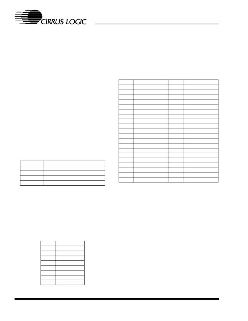
�J13� -� MII� Connector� (Table� 3).�
�Background� Information�
�Pin�
�1�
�Function�
�MII� Power�
�Pin�
�21�
�Function�
�MII� Power�
�?�
�?�
�IEEE� Std� 802.3u-1995� (ISO/IEC� 8802.3:1996)�
�CSMA/CD� Access� Method� and� Physical� Layer�
�Specifications�
�IEEE� Std� 802.3u-1995� Supplement� Clause� 28�
�(Auto-� N� egotiation)�
�2�
�3�
�4�
�5�
�6�
�7�
�8�
�MDIO�
�MDC�
�RXD3�
�RXD2�
�RXD1�
�RXD0�
�RX_DV�
�22�
�23�
�24�
�25�
�26�
�27�
�28�
�Ground�
�Ground�
�Ground�
�Ground�
�Ground�
�Ground�
�Ground�
�?�
�CS8952� CrystalLAN� TM�
�10Base-T�
�and�
�9�
�RX_CLK�
�29�
�Ground�
�100Base-X� Transceiver� Datasheet�
�Evaluation� Kit� Contents�
�The� CDB8952� Evaluation� Board� Kit� includes� the�
�following:�
�10�
�11�
�12�
�13�
�14�
�15�
�RX_ER/RXD4�
�TX_ER/TXD4�
�TX_CLK�
�TX_EN�
�TXD0�
�TXD1�
�30�
�31�
�32�
�33�
�34�
�35�
�Ground�
�Ground�
�Ground�
�Ground�
�Ground�
�Ground�
�Quantity� Item�
�1� CDB8952� Evaluation� Board�
�1� CS8952� Datasheet�
�1� CDB8952� Reference� Manual�
�1� CDB8952� Kit� Packing� List�
�Table� 1.� Evaluation� Kit� Contents�
�16�
�17�
�18�
�19�
�20�
�TXD2� 36�
�TXD3� 37�
�COL� 38�
�CRS� 39�
�MII� Power� 40�
�Table� 3.� MII� Connector�
�Ground�
�Ground�
�Ground�
�Ground�
�MII� Power�
�BOARD� CONFIGURATION�
�I/O� Connectors�
�J1� -� External� TX_CLK.� This� connector� may� be�
�used� to� supply� TX_CLK� when� HDR42� and� HDR43�
�are� set� appropriately.�
�J2� -� RJ45,� Twisted-pair� Media� (Table� 2).�
�Pin� Function�
�1� TD+�
�2� TD-�
�Configuration� Jumpers� and� Switches�
�S1� -� Board� Reset.� Depressing� this� push-button�
�switch� will� force� the� CS8952� into� a� reset� state.�
�S2� -� Test� 1� (not� populated).� This� switch� is� used� to�
�select� a� factory� test� mode,� and� should� not� be�
�pressed� during� normal� operation.�
�S3� -� Physical� Address� Select.� This� 5-position�
�switch� is� used� to� select� the� physical� address� to�
�which� the� CS8952� will� respond.� “Open”� or� “Off”�
�3�
�4�
�5�
�6�
�7�
�8�
�RD+�
�-�
�-�
�RD-�
�-�
�-�
�will� set� the� corresponding� physical� address� bit� to�
�ZERO,� while� “Closed”� or� “On”� will� set� it� to� ONE.�
�The� CS8952� checks� the� positions� of� this� switch�
�only� during� power-up� or� reset.� If� any� switch� posi-�
�tion� is� changed,� a� reset� or� power� cycle� is� required�
�Table� 2.� Twisted-pair� Media�
�before� the� new� settings� will� take� effect.�
�CIRRUS� LOGIC� ADVANCED� PRODUCT� DATABOOK�
�2�
�DS206DB2�
�发布紧急采购,3分钟左右您将得到回复。
相关PDF资料
CDCE906-706PERFEVM
EVAL MOD PERFORMANCE CDCE906/706
CEVAL-033
BOARD EVAL FOR CVCO33 .3"X.3"
CF37S
COVER FLANGE 37POS FEMALE
CG0402MLC-05LG
SUPPRESSOR ESD 5VDC 0402 SMD
CG0402MLU-24G
SUPPRESSOR ESD 24VDC 0402 SMD
CG0603MLA-26KE
CHIP GUARD
CG0603MLD-12E
VARISTOR 12VDC 1CH 0603 SMD
CG0603MLE-18E
CHIP GUARD
相关代理商/技术参数
CDB-9PF
制造商:HRS 制造商全称:HRS 功能描述:CD CRIMP TYPE CONNECTOR
CDB-9SF
制造商:HRS 制造商全称:HRS 功能描述:CD CRIMP TYPE CONNECTOR
CDBA1100
制造商:COMCHIP 制造商全称:Comchip Technology 功能描述:SMD Schottky Barrier Rectifier
CDBA1100-G
功能描述:肖特基二极管与整流器 SCHOTTKY DIODE 1A, 100V RoHS:否 制造商:Skyworks Solutions, Inc. 产品:Schottky Diodes 峰值反向电压:2 V 正向连续电流:50 mA 最大浪涌电流: 配置:Crossover Quad 恢复时间: 正向电压下降:370 mV 最大反向漏泄电流: 最大功率耗散:75 mW 工作温度范围:- 65 C to + 150 C 安装风格:SMD/SMT 封装 / 箱体:SOT-143 封装:Reel
CDBA1100GS
制造商:COMCHIP 制造商全称:Comchip Technology 功能描述:SMD Schottky Barrier Rectifier
CDBA1100-HF
制造商:COMCHIP 制造商全称:Comchip Technology 功能描述:SMD Schottky Barrier Rectifiers
CDBA1100LR-HF
制造商:COMCHIP 制造商全称:Comchip Technology 功能描述:Low VF Low IR SMD Schottky Barrier Rectifiers
CDBA1150-G
功能描述:肖特基二极管与整流器 150V, 1A RoHS:否 制造商:Skyworks Solutions, Inc. 产品:Schottky Diodes 峰值反向电压:2 V 正向连续电流:50 mA 最大浪涌电流: 配置:Crossover Quad 恢复时间: 正向电压下降:370 mV 最大反向漏泄电流: 最大功率耗散:75 mW 工作温度范围:- 65 C to + 150 C 安装风格:SMD/SMT 封装 / 箱体:SOT-143 封装:Reel